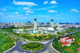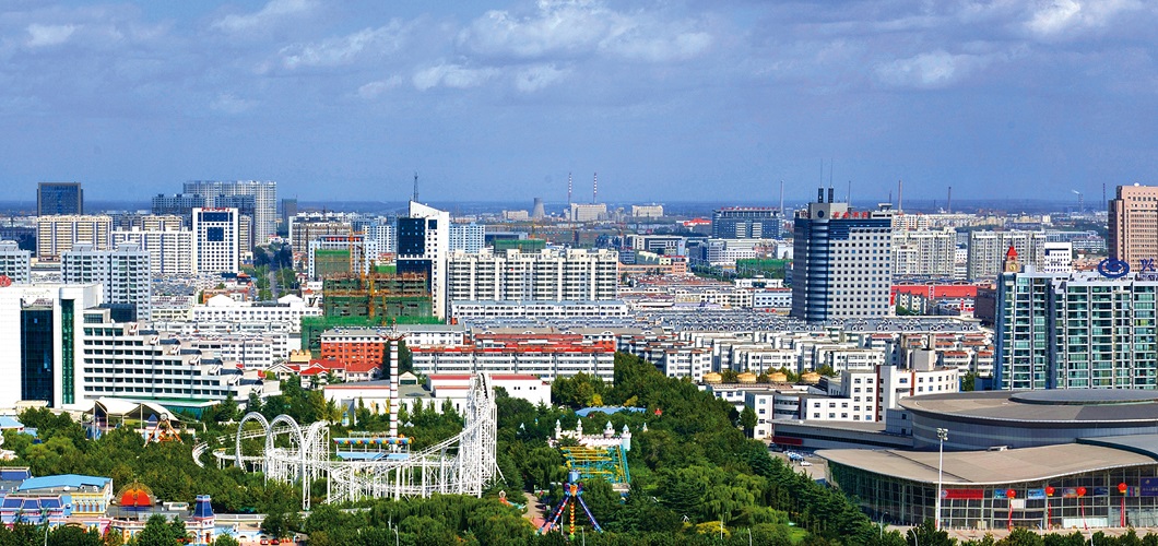
Weifang Optoelectronics Industrial Park

Weifang Optoelectronics Industrial Park is located in Weifang National Hi-tech Industrial Development Zone. It is a research and development base for technology companies and institutions specializing in optoelectronics and electro-acoustics.
With an investment of 20 billion yuan, the industrial park has a planned development area of 3 million square meters.
Weifang Optoelectronics Industrial Park has been awarded with several national and provincial titles, including National Semiconductor Lightings Engineering Industrialization Base and Shandong Information Technology Industrial Park. In 2011, Weifang Optoelectronics Industrial Park was authorized as the only luminescent semiconductor industry cluster in China. In 2013, it was listed as one of the top 10 innovative industrial clusters supported by the Ministry of Science and Technology, signifying that the park has shouldered the responsibility of developing strategic emerging industries in China.
Weifang Optoelectronics Industrial Park has attracted over 130 high-end talents, including one talent from the Recruitment Program of Global Experts and two talents of the Taishan Scholars Program of Shandong Province. They work for the two main industrial chains in the park—an industrial chain of semiconductors and an industrial chain of electro-acoustic devices.
As the country's largest electro-acoustic products distribution center, the total output value of the industrial park reached 22 billion yuan ($3.25 billion) in 2014. The profits and taxes were 3.5 billion yuan. At present, there are more than 200 enterprises operating in the park making products for Apple, Samsung, LG, Sony, Plantronics, Microsoft, Huawei, Lenovo and other well-known international companies.
Advanced Optronic Devices (China) Co, one of the enterprises calling the park its home, operates a business in optical lighting, optical information, optical life, optical film, optical capital and other optical industrial fields. The company has delivered more than 600 thousand outdoor LED lights and more than 5 million indoor LED lights to more than 32 countries and territories.
Weifang YiTong Electronics Co, another enterprise in the park, is engaged in the production of electric vibrating membranes, back plates, film capacitors, high temperature materials PI film, flexible circuit board materials and piezoelectric film.
The construction of Weifang Optoelectronics Industrial Park was divided into two phases. The first phase covered an area of 1.3 million square meters with an investment of 10 billion yuan. The phase contained two incubators and three accelerators of optoelectronic technology enterprises.
The second phase, with a planning area of more than 1.7 million square meters, garnered a total investment of 12 billion yuan. The main body of the second phase is Goertek Inc, a company focusing on R&D, production and sales of electro-acoustic components, optical components, electronic accessories and related products.
Science and technology service platforms are also founded in the park, such as Weifang 3D Printing Technology Innovation Center and Weifang Testing Center of Semiconductor Lighting Products, in order to provide convenience for the enterprises in the park.
Weifang Testing Center of Semiconductor Lighting Products is a science and technology service platform set up by the Management Committee of Weifang High-tech Zone. The testing center has an area of 4,000 square meters with an investment of 70 million yuan.
The testing center mainly examines the reliability and safety of products such as semiconductor devices, semiconductor lighting, LED displays, LCM module and electro acoustics. It obtained the certificate of China National Accreditation of Laboratories (CNAS) in July, 2014. In June, 2015, the testing center passed the supervision and on-site assessment of CNAS.
Weifang 3D Printing Technology Innovation Center is an advanced manufacturing integrated service platform established by the Management Committee of Weifang High-tech Zone and China Academy of Machinery Science & Technology. It has an area of 7400 square meters with an investment of 100 million yuan.
The center integrates the production, study, research and application of 3D printing technologies. There is an integrated service system of industrial services, creative design, bio-medical treatment and a popular science plaza.
Gathering high-quality resources from China and the world, Weifang Optoelectronics Industrial Park promises to be a wellspring of innovative photoelectron and electro-acoustic products, focusing on the areas of sapphire substrate, epitaxial wafer growth, chip preparation, device packaging, optical communications, electro-acoustic devices and consumer electronics.
Optoelectronics, generally considered a sub-field of photonics, is the study and application of electronic devices and systems that source, detect and control light. In this context, light often includes invisible forms of radiation, such as gamma rays, X-rays, ultraviolet and infrared, in addition to the visible light spectrum. Optoelectronic devices are electrical-to-optical or optical-to-electrical transducers, or instruments that use such devices in their operations. Electro-optics is often erroneously used as a synonym, but is a wider branch of physics that concerns all interactions between light and electric fields, whether or not they form part of an electronic device.
Location:Gaoxin Building at the crossroads of Yuqing East Street and Dongfang Road
Investment promotion:2999006
Incubators managment: 2999007
Industrial Park administration:2999020
Integrated management:2999080
Weifang Inspection Center of LED Product:5070356
3D Printing Technology Innovation Center of Weifang:2225108